Abrupt PN junction at thermal equilibrium
A PN junction is the juxtaposition of a n-type and a p-type piece of semiconductor, taken originally from the same block of crystal. The difference between the densities of donors and acceptors ND - NA undergoes a very sharp variation from a negative value in the P region to a positive value in the N region. An abrupt junction is by definition a junction in which the doping type changes over a very small distance compared to the spatial extent of the depletion region (see below.)

![[zoom...]](javascript:window.open(%22../res/k_fig_01_1.jpg%22,%22_blank%22,%22width=%22+Math.min(800,screen.availWidth)+%22,height=%22+Math.min(600,screen.availWidth)+%22,left=%22+(screen.availWidth-800)/2+%22,top=%22+(screen.availHeight-600)/2+%22,scrollbars=yes,resizable=yes%22)?void(0):void(0))
There are some other types of junctions (exponential, linear junctions...). However we will only focus here on the abrupt junction, because results are much simpler and can be easily generalized to more complex cases.
![[zoom...]](javascript:window.open(%22../res/k_fig_02_1.jpg%22,%22_blank%22,%22width=%22+Math.min(800,screen.availWidth)+%22,height=%22+Math.min(600,screen.availWidth)+%22,left=%22+(screen.availWidth-800)/2+%22,top=%22+(screen.availHeight-600)/2+%22,scrollbars=yes,resizable=yes%22)?void(0):void(0))
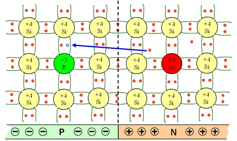
Figure EC2 enables understanding what happens when a N-type semiconductor is in contact with a P-type semiconductor. The electrons, abundant in the N-type region, will cross the junction in order to recombine with holes present in the P-type region. Therefore, a negative static space charge builds up in the P region (the trivalent boron atoms have a static negative charge since they release a positively-charged hole in the valence band) whereas a positive space charge builds up in the N-type zone for the same reasons. The small volume in which this space charge is created is called the space charge zone or depletion zone. Because there is a strong electric field in this area, the density of free carriers is negligible at thermal equilibrium. In addition, the frontier between the depletion zone and the neutral parts of the junction is very sharp.
![[zoom...]](javascript:window.open(%22../res/k_fig_03_1.jpg%22,%22_blank%22,%22width=%22+Math.min(800,screen.availWidth)+%22,height=%22+Math.min(600,screen.availWidth)+%22,left=%22+(screen.availWidth-800)/2+%22,top=%22+(screen.availHeight-600)/2+%22,scrollbars=yes,resizable=yes%22)?void(0):void(0))
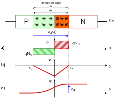
Just after the P- and N-type semiconductors have been drawn closer, a potential barrier appears for both holes an electrons. Indeed, the static space charges accumulated at the borders of the junction (positive charges in the N zone, negative charges in the P zone) create an electric field pointing from N towards P, which prevents diffusion and further recombination of electrons and holes: diffusion is then rapidly stopped by the buildup of this internal electric field. In addition, because of the existence of this double layer of charges on both sides of the junction, the electrostatic potential varies sharply inside the depletion zone and the potential difference Vd, called the diffusion potential (or built-in potential) reaches non-negligible values (e.g. 0.8V for Si). However, if we attempt to measure a voltage by connecting a multimeter at both sides of the PN diode, we will find a zero voltage drop, because a multimeter measures a difference in electrochemical potentials, not just electrostatic potentials. Indeed, here the electrochemical potential is constant throughout the crystal, including in the space charge zone, because this potential takes into account not only the electric field but also the concentration gradient of charge carriers. The diffusion potential due to this gradient compensates exactly for the electrostatic potential.
The relationship between the space
 charge density , the electric field
 and the electrostatic potential
 is :
is :
Where
 is the permittivity of the medium (10‑10 F/m for silicon).
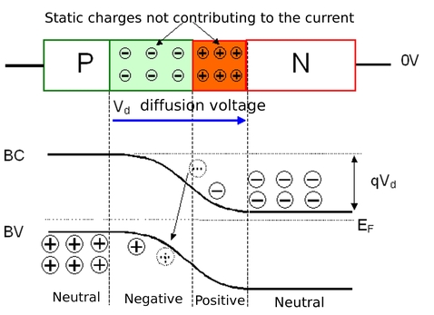
The (chemical) potential of a semiconductor being equal to its Fermi energy, the built-in potential or diffusion potential is proportional to the difference of the Fermi energies of the two unbounded semiconductors :
When the junction meets thermal equilibrium, the Fermi energy has a constant value throughout the whole device. The energies of conduction and valence bands are therefore shifted up or down, and exhibit a smooth variation across the depletion region. As a consequence, there is an electrostatic potential energy difference appearing between the P and N region, equal to qVd.
![[zoom...]](javascript:window.open(%22../res/k_fig_04_1.jpg%22,%22_blank%22,%22width=%22+Math.min(800,screen.availWidth)+%22,height=%22+Math.min(600,screen.availWidth)+%22,left=%22+(screen.availWidth-800)/2+%22,top=%22+(screen.availHeight-600)/2+%22,scrollbars=yes,resizable=yes%22)?void(0):void(0))