CCD working
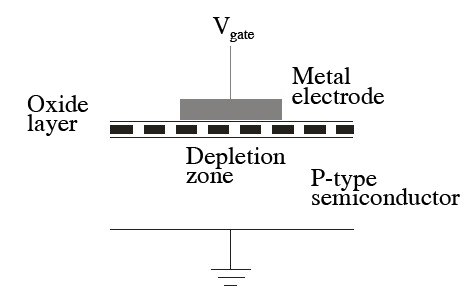
The technology on which CCD sensors are based is the MOS capacitor (Metal Oxide Semiconductor) (Fig.3). If a photon, whose energy exceeds the energy of the gap, is absorbed in the depletion zone, it creates an electron-hole pair. The electron remains in the depletion zone while the hole heads toward the earth electrode. The amount of negative charge (electrons) that can be collected is proportional to the voltage applied, the oxide thickness and to the surface of the gate electrode. The total number of electrons that can be stored is called “well capacity”. When the wavelength increases, photons are absorbed at increasing depths. It notably limits the response to high wavelengths. Currently, available sensors can function from far infrared to X-rays.
![[zoom...]](javascript:window.open(%22../res/Fig_03_1.jpg%22,%22_blank%22,%22width=%22+Math.min(800,screen.availWidth)+%22,height=%22+Math.min(600,screen.availWidth)+%22,left=%22+(screen.availWidth-800)/2+%22,top=%22+(screen.availHeight-600)/2+%22,scrollbars=yes,resizable=yes%22)?void(0):void(0))
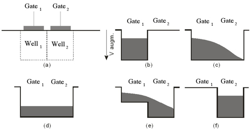
The CCD register consists of a serie of gates. The handling of gate voltage, in a systematic and sequential way, transfers the electrons from one gate to another like a courier. For the charge transfer, depletion zones have to overlap each other(Fig 4.a). Depletion zones are in gradient and gradients should overlap so that the charge transfer occurs.
Each gate has its own control voltage that varies according to time. Voltage is a squarewave signal called “clock” or “clock signal”. First, a voltage is applied at gate 1 and photoelctrons are collected in the well 1 (b). When a voltage is applied at gate 2, electrons move toward well 2 like a waterfall (c). This process is fast and charge is rapidly balanced between the two wells (d). When the voltage is reduced at the gate 1, the potential well decreases and all the electrons flow again cascading into well 2 (e). Finally, when the voltage applied at gate 1 approaches zero, all the electrons are in the well 2 (f). This process is repeated several times until the charge is transferred across all the shift register. When the gate voltage is low, it acts as a barrier whereas when the voltage is high, the charge can be stored.
A pixel can be constituted of several gates (from 2 to 4, or even more), sometimes also called system phases. According to the clock signals (cf. infra), and for an equal pixel size, 50% of the pixel surface is available for the well with a four-phases system, to 33% with a three-phases system.
![[zoom...]](javascript:window.open(%22../res/Fig_04_1.jpg%22,%22_blank%22,%22width=%22+Math.min(800,screen.availWidth)+%22,height=%22+Math.min(600,screen.availWidth)+%22,left=%22+(screen.availWidth-800)/2+%22,top=%22+(screen.availHeight-600)/2+%22,scrollbars=yes,resizable=yes%22)?void(0):void(0))
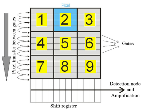
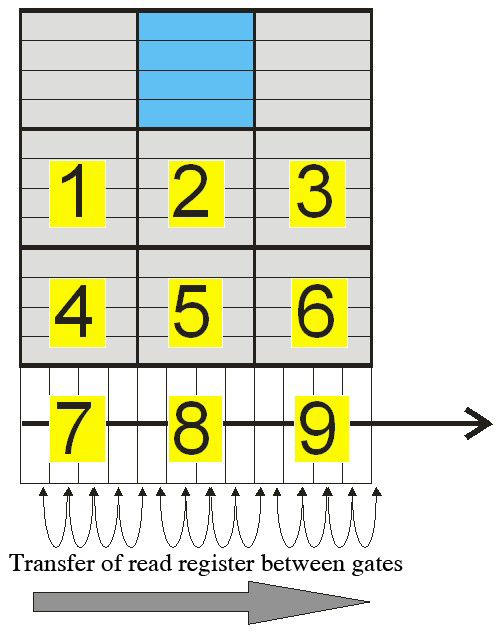
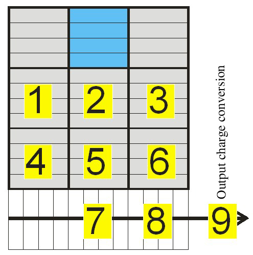
The CCD matrix is a series of registers in columns (Fig. 5). After exposure and charge generation by photoelectric effect for each pixel, the charge is stored in the lines or in the columns by channels or arrest blocks and depletion zones overlap only in one direction (descendant for columns, horizontal for the reading line). Charge transfer first occurs from line to line by intra and then inter-pixel gate jumps (Fig. 6). At the end of each column, there is an horizontal pixel register. This register collects one line at a time and then transports the charge packets in serial mode to an output amplifier. The entire horizontal serial register has to be synchronized with the detection node before the next line enters the serial register (Fig. 6). That's why separated vertical and horizontal clocks are required for all matrices.
![[zoom...]](javascript:window.open(%22../res/Fig_05_1.jpg%22,%22_blank%22,%22width=%22+Math.min(800,screen.availWidth)+%22,height=%22+Math.min(600,screen.availWidth)+%22,left=%22+(screen.availWidth-800)/2+%22,top=%22+(screen.availHeight-600)/2+%22,scrollbars=yes,resizable=yes%22)?void(0):void(0))
![[zoom...]](javascript:window.open(%22../res/Fig_06_1.jpg%22,%22_blank%22,%22width=%22+Math.min(800,screen.availWidth)+%22,height=%22+Math.min(600,screen.availWidth)+%22,left=%22+(screen.availWidth-800)/2+%22,top=%22+(screen.availHeight-600)/2+%22,scrollbars=yes,resizable=yes%22)?void(0):void(0))
![[zoom...]](javascript:window.open(%22../res/Fig_07_1.jpg%22,%22_blank%22,%22width=%22+Math.min(800,screen.availWidth)+%22,height=%22+Math.min(600,screen.availWidth)+%22,left=%22+(screen.availWidth-800)/2+%22,top=%22+(screen.availHeight-600)/2+%22,scrollbars=yes,resizable=yes%22)?void(0):void(0))
The interaction between thousands of transfers reduces the output signal. The capacity to transfer the charge is specified by the charge transfer efficiency (CTE). Although one can use any number of transfer sites (gates) by pixel on the sensor surface, we generally use from two to four of them, or even a virtual phase system that only requires one clock.
In each mentioned system, the final step of the process consists in the conversion of the charge packet into a measurable voltage. This is achieved by a floating diode or a floating diffusion. The diode, working as a capacitor, generates a voltage proportional to the number of electrons, ne. Then, the signal can be amplified, processed and digitally encoded by electronic processor independent from the CCD sensor.
With several matrices, it is possible to move more than one charge line in the serial register. Similarly, it is also possible to move more than one element from the serial register into a summing gate just before the output node. It is called “binning”, “super pixeling”, or even “charge gathering”. The binning increases the output signal and the signal dynamic range, but at the expense of the sensor spatial resolution. As it increases the signal-to-noise ratio, the binning is interesting for low-light-level applications in cases in which resolution is not really important. Serial registers and output nodes require wells of higher capacity for binning. If the output capacitor is not updated after each pixel, then it can accumulate charge.