Current density
In order to describe the behavior of a semiconductor out of thermal equilibrium (upon application of an external voltage), we have to estimate the electrical currents resulting from the motion of charge carriers. The latter, electrons and holes, will move because either an electric field is applied, or because a concentration gradient of charge carriers exists. In the first case, the current is called a conduction current, while in the second case it is called a diffusion current. Moreover, it is more relevant to consider a current density J (which is a current, i.e. an amount of charges per unit time, per unit area) instead of the current itself.
When electrons and holes are submitted to an electric field created by an applied voltage, their flow generates a conduction current :
Where n (p) is the electron (hole) density, q=1,602.10-19C is the electron elementary charge, E is the electric field of the polarized junction, and µn et µp are the mobilities of electrons and holes, respectively.
Besides, when electron and hole densities do not have constant values throughout the semiconductor, there is a diffusion flow that tends to flatten the density profile. This diffusion current is proportional to the concentration gradient :
Where Dn and Dp are the diffusion constants of both types of carriers.
The electron mobility being higher than that of holes, the Einstein relationship shows that, for a given concentration gradient, the diffusion current for electrons is higher than the diffusion current for holes.
It is obvious that the total current is constant throughout the whole device. Then, in an attempt to estimate this current, we may choose a region in which calculations will be as simple as possible. This region corresponds to the neutral parts of the N and P sections. Indeed, the electric field
 , in the low injection regime, is negligible out of the depletion zone, in virtue of the non-zero conductivity of semiconductors (if the field was not zero, free charges would escape and the region would not be neutral any more.) The total current is therefore only the combination of the hole and electron diffusion currents. But, in neutral zones (out of the depletion zone), the spatial distribution of majority carriers (electrons in the N part, holes in the P part) is constant. Therefore, since diffusion currents are proportional to carrier concentration gradients, the total current turns out to be generated by minority carriers, i.e. electrons in the P side and holes in the N side. The expression of the total current density is then :
Where xp (resp. xn) is the limit of the depletion zone in the P side (resp. N side.)

![[zoom...]](javascript:window.open(%22../res/k_fig_05_1.jpg%22,%22_blank%22,%22width=%22+Math.min(800,screen.availWidth)+%22,height=%22+Math.min(600,screen.availWidth)+%22,left=%22+(screen.availWidth-800)/2+%22,top=%22+(screen.availHeight-600)/2+%22,scrollbars=yes,resizable=yes%22)?void(0):void(0))
In order to calculate J as a function of the external voltage V, we have to estimate the minority carriers densities np (=n(xp)) and pn (=p(xn)) in the neutral zones. To do so, we have to write the continuity equations giving the evolution of the carrier densities versus time.
![[zoom...]](javascript:window.open(%22../res/k_fig_06_1.jpg%22,%22_blank%22,%22width=%22+Math.min(800,screen.availWidth)+%22,height=%22+Math.min(600,screen.availWidth)+%22,left=%22+(screen.availWidth-800)/2+%22,top=%22+(screen.availHeight-600)/2+%22,scrollbars=yes,resizable=yes%22)?void(0):void(0))
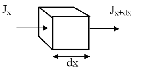
Let's consider an infinitesimally small volume of semiconductor of unit section area and length dx. Let np (resp. pn) be the electron density in the P side (resp. the hole density in the N side.) The number of carriers in the small volume can change because the current density is not homogeneous in space (there are more or less charges exiting the volume than entering the same volume: the variation per unit time is equal to
 ), or because carriers have recombined (which is described by a lifetime
 or
or
 ). We do not allow carriers to be generated here. We then obtain the following charge conservation equations :
Where np0 = n(xp) (resp. pn0 = p(xn)) is the electron density (resp. hole density) in the P side (resp. N) for the passive junction, and
,
are the lifetimes of the carriers in neutral regions.
The steady-state continuity equations write :
Where
 is the diffusion length of electrons/holes.
The expression of the diffusion potential (see above) can be written as a relationship between the densities of minority carriers (np0 and pn0) and majority carriers nn0 (=ND) and pp0 (=NA), for the junction at thermal equilibrium :
When the junction is connected to an external forward voltage source V, the electrostatic potential difference becomes Vd –V. Like in the junction at thermal equilibrium, the majority and minority carriers densities are linked by :
In the low injection regime, the densities of majority carriers remain almost constant whatever the forward voltage applied to the diode; however it is not the case for minority carriers :
We are now able to solve the steady-state differential continuity equations; for this purpose boundary conditions have to be determined. Applying an external bias on the device cannot modify the density of minority carriers far from the junction, which can be written as :
 and
and
 . The variations in minority carriers density can be written as a function of the position x inside the junction, out of the depletion zone :
Since the current is constant through the whole device, it can be calculated for instance at the boundaries of the depletion zone. The total current density across the diode is :
With