Size and architecture
Choice criteria can entirely depend on the laboratory's application, budget or history. Althought there is no general rule, a specific type of device can often be linked with a specific type of laboratory:
-
Scientific applications: block transfer,
-
Television and mass market: interline transfer,
-
Industrial applications: linear sensors, progressive scan, TDI, ...
-
Military applications: anything useful ...
Scientific applications often deal with high spatial or temporal resolution or high greyscale resolution. Mass market application mainly have to be compatible with high-contrast images.
Noise is not a great concern for the general public, but for professional applications involving numerous relays, noise has to be reduced to a minimum. For industrial applications, the context and the application itself dictate the choice of lighting and sensors; The cost is also a concern for many laboratories. For military applications, everything has to contribute to the final goal: visualization of the desired phenomenon, no matter at what cost.
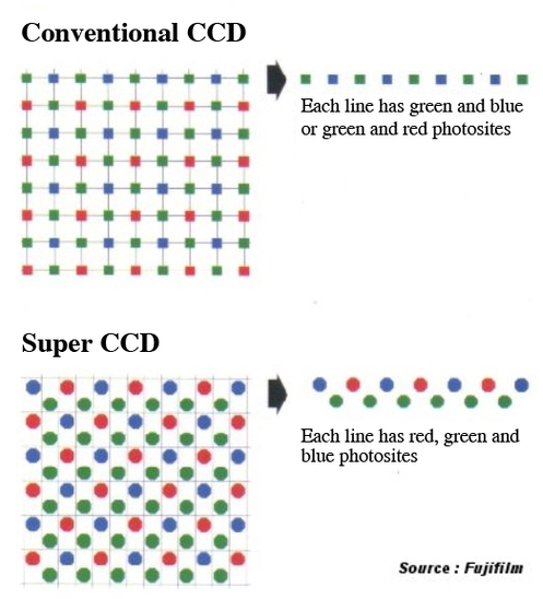
During the last decade, from the geometrical point of view, manufacturers focused on maximizing the fill ratio and thus on covering the image space with as much sensitive pixels as possible. However, an increase in the number of pixels for a better resolution leads to an increase in the signal-to-noise ratio and a decrease in sensitivity and exposure latitude due to the pixels being smaller. Super-CCD solve these problems and improve the quality of the final image.
In the year 2000, the first Super-CCD were created to improve performance. Further generations were to improve resolution, and the next tends to increase sensitivity.
![[zoom...]](javascript:window.open(%22../res/Fig_22_1.jpg%22,%22_blank%22,%22width=%22+Math.min(800,screen.availWidth)+%22,height=%22+Math.min(600,screen.availWidth)+%22,left=%22+(screen.availWidth-800)/2+%22,top=%22+(screen.availHeight-600)/2+%22,scrollbars=yes,resizable=yes%22)?void(0):void(0))
SR Super-CCD created by Fuji radically extend exposure latitude and improve sensitivity thanks to two different types of sensors contained in its photosites.
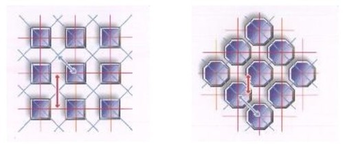
The octagonal photodiode (Fig. 22) and the honeycomb disposition allowed a greater display surface for each photosite. The surface of one photodiode in a ½ inch, 3-million pixel Super-CCD is 2.3 times the surface of a same-size conventional CCD. Thus sensitivity, signal-to-noise ratio and exposure latitude could be improved. Honeycomb disposition of the pixels also allows to get closer to the human sight's image quality.

![[zoom...]](javascript:window.open(%22../res/Fig_23_1.jpg%22,%22_blank%22,%22width=%22+Math.min(800,screen.availWidth)+%22,height=%22+Math.min(600,screen.availWidth)+%22,left=%22+(screen.availWidth-800)/2+%22,top=%22+(screen.availHeight-600)/2+%22,scrollbars=yes,resizable=yes%22)?void(0):void(0))
![[zoom...]](javascript:window.open(%22../res/Fig_24_1.jpg%22,%22_blank%22,%22width=%22+Math.min(800,screen.availWidth)+%22,height=%22+Math.min(600,screen.availWidth)+%22,left=%22+(screen.availWidth-800)/2+%22,top=%22+(screen.availHeight-600)/2+%22,scrollbars=yes,resizable=yes%22)?void(0):void(0))
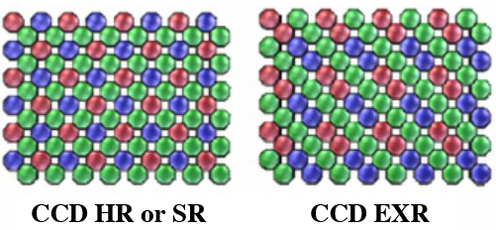
Super-CCD HR offer far better resolution. A pixel is interpolated between each pair of sensors. Another useful property is the fineness of their electrodes, which reduces the depth of photosite pits. Thus photosite receive more light. Furthermore, Super-CCD are still being developed. The Super-CCD SR and Super-CCD EXR models, for instance, combine the properties of the two previous models and create an image with a quality almost comparable to that of the human eye.
Traditionally, there is only one photodiode for each photosite to capture the whole light range. Super-CCD SR have two different types of photodiodes for each photosite. (Fig 25).
Thus, photosites are doubled. S photodiodes are highly sensitive but have a narrow exposure latitude. They capture dark and mildly clear colors. On the other hand, R photodiodes are less sensitive (i.e. they record a darker image) but can spot details in clearer areas, contrary to conventional photodiodes.
The combination of those two photodiodes allows an exposure latitude four times as wide as that of a conventional photodiode. This creates a more detailed image, especially in darker and lighter zones.

![[zoom...]](javascript:window.open(%22../res/Fig_25_1.jpg%22,%22_blank%22,%22width=%22+Math.min(800,screen.availWidth)+%22,height=%22+Math.min(600,screen.availWidth)+%22,left=%22+(screen.availWidth-800)/2+%22,top=%22+(screen.availHeight-600)/2+%22,scrollbars=yes,resizable=yes%22)?void(0):void(0))
Furthermore, the augmentation of the sensor's exposure latitude (or dynamic range) allows incorrect exposition up to a certain point (i.e. more tolerance for poor lighting conditions, over or underexposure). There are two generations of Super-CCD SR exploiting the same principle but with a different disposition for the photodiodes. In the first version, each photosite is divided in two to be able to contain both photodiodes. In the second version, the S photodiode occupies the whole surface of the photosite and the R photodiode is placed between the octagonal photosites. This technique allows greater sensitivity, because the photodiode surface is greater in SR II than in SR.
The Super-CCD EXR sensor was revealed in 2008 and is the result of a combination between the properties of Super-CCD HR and Super-CCD SR. It consists of a three-in-one universal sensor with very high resolution, high sensitivity and a wide exposure latitude, thus radically improving image quality.
The Super-CCD EXR can be adjusted to the object which is being photographed to obtain the best possible image. This sensor comports three main modifications compared to the previous generations.
-
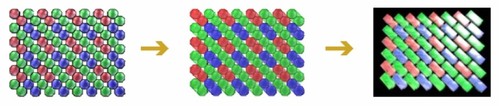
First, color filters are disposed differently upon the matrix.
![[zoom...]](javascript:window.open(%22../res/Fig_26_1.jpg%22,%22_blank%22,%22width=%22+Math.min(800,screen.availWidth)+%22,height=%22+Math.min(600,screen.availWidth)+%22,left=%22+(screen.availWidth-800)/2+%22,top=%22+(screen.availHeight-600)/2+%22,scrollbars=yes,resizable=yes%22)?void(0):void(0))
This new disposition is an answer to the need of noise reduction. To increase sensitivity, the sensor's output electronic gain has to be amplified but this procedure also increases noise. Noise can also be reduced by grouping pixels (pixel binning). Binning is often done by grouping pixels horizontally or vertically,generating flaws by increasing space between same-colour grouped pixels. Correcting these flaws greatly reduces resolution.
For Super-CCD EXR, the disposition of color filters allows a diagonal blooming (a technology called “close incline pixel coupling”) and avoids flaws created by inter-pixel space.
This blooming technique doubles the sensitive element's surface and thus increases sensitivity while keeping noise to a minimum.
![[zoom...]](javascript:window.open(%22../res/Fig_27_1.jpg%22,%22_blank%22,%22width=%22+Math.min(800,screen.availWidth)+%22,height=%22+Math.min(600,screen.availWidth)+%22,left=%22+(screen.availWidth-800)/2+%22,top=%22+(screen.availHeight-600)/2+%22,scrollbars=yes,resizable=yes%22)?void(0):void(0))
-
Another benefit of Super-CCD EXR compared to previous generation sensors is its high exposure latitude. This sensor can perceive two different images for a same object: one in high sensitivity, the other in low sensitivity. With the same technology as the Super-CCD SR, the EXR uses Dual Exposition Control. Two same-color adjacent pixels have different sensitivities (high for one half of the sensor's photodiodes and low for the other half). This can be done by controlling the exposure time of photodiodes. A pixels have a 1-100th of a second obturation time whereas it is 1-400th of a second for B pixels. Thus A pixels record details in dark tones whereas B pixels record clear shades. The combination of both renderings helps maintain a good lighting on the whole image.
Contrary to SR sensors, the photodiodes in EXR sensors are all the same size for a wider exposure latitude and greater sensitivity.

![[zoom...]](javascript:window.open(%22../res/Fig_28_1.jpg%22,%22_blank%22,%22width=%22+Math.min(800,screen.availWidth)+%22,height=%22+Math.min(600,screen.availWidth)+%22,left=%22+(screen.availWidth-800)/2+%22,top=%22+(screen.availHeight-600)/2+%22,scrollbars=yes,resizable=yes%22)?void(0):void(0))
-
The third property of Super-CCD EXR is high resolution. Its structure allows the use of all pixels and its processor optimizes the signal processing to obtain the highest possible resolution. Even though it was primarily designed to have a greater sensitivity (and pixel grouping), the image quality is the same as with other 12-mega-pixel sensors.
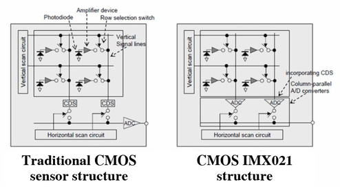
CMOS sensors technology (cf. infra) also evolves in terms of geometry. In one of the last generations, photodiodes have been rotated 45° to obtain a resolution 1,4 times as high as that of a conventional CMOS sensor with the same properties. Thanks to this new structure, the IMX021 generation of CMOS sensors generates high-quality images with low noise.
As for Sony Exmor R sensors, their photodiodes are placed differently than for conventional sensors. They are found just below the color filter for a greater sensitivity and much lower noise.
![[zoom...]](javascript:window.open(%22../res/Fig_29_1.jpg%22,%22_blank%22,%22width=%22+Math.min(800,screen.availWidth)+%22,height=%22+Math.min(600,screen.availWidth)+%22,left=%22+(screen.availWidth-800)/2+%22,top=%22+(screen.availHeight-600)/2+%22,scrollbars=yes,resizable=yes%22)?void(0):void(0))

![[zoom...]](javascript:window.open(%22../res/Fig_30_1.jpg%22,%22_blank%22,%22width=%22+Math.min(800,screen.availWidth)+%22,height=%22+Math.min(600,screen.availWidth)+%22,left=%22+(screen.availWidth-800)/2+%22,top=%22+(screen.availHeight-600)/2+%22,scrollbars=yes,resizable=yes%22)?void(0):void(0))